

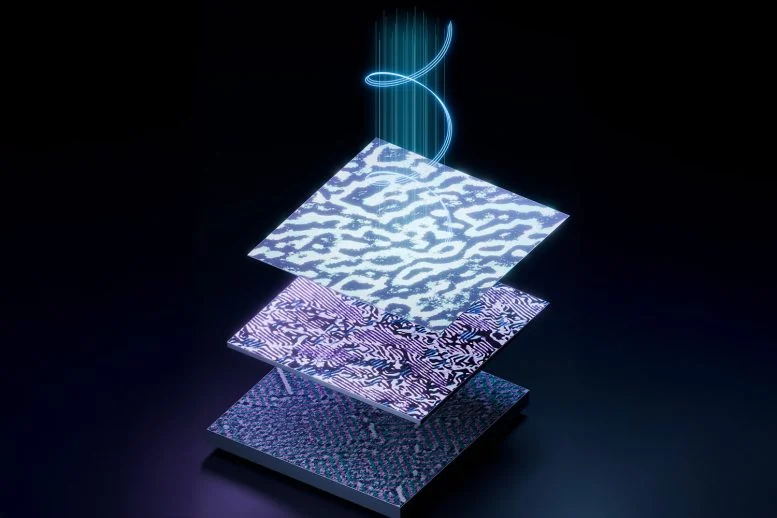
Breakthrough in Multiferroic Materials Could Transform Ultra-Low-Power Computing
Researchers at Brown University have made significant strides in the development of multiferroic materials for ultra-low-power computer chips, overcoming a major barrier that has limited their application in modern electronics.
A new class of materials is poised to vastly reduce electricity consumption in computing, but a recurring challenge has hindered their integration into computer chips. When these materials are manufactured in thin formats suitable for electronics, their valuable electrical and magnetic properties often diminish.
In a recent study published in Nature Materials, the Brown research team unveiled a method that enables the production of ultrathin films of bismuth ferrite, a type of multiferroic material that retains its essential characteristics. This innovative approach also results in an enhanced form of magnetism, promising benefits for future computing applications.
Understanding the Limitations of Multiferroic Materials
Bismuth ferrite belongs to a unique category of materials known as multiferroics, which possess intertwined electrical and magnetic attributes. The crystalline structure of these materials leads to the displacement of positive and negative charges in opposite directions, which generates electrical polarization. By applying a small voltage, this polarization can be reversed, allowing information to be encoded as binary data (0s and 1s). This linkage between electrical and magnetic states could potentially enable energy-efficient memory and logic devices.
However, the performance of these multiferroic films is often compromised by the “dead layer” effect. When the films are produced at extremely thin scales, their atomic structures and chemical environments can become unstable, disrupting their functionalities. Concurrently, internal electric fields can destabilize the material’s polarization, eroding the necessary ferroelectric and magnetic characteristics for electronic usage.
Innovative Engineering Solutions to Overcome Dead Layers
The team at Brown University tackled these issues by expertly engineering the layers that envelop the bismuth ferrite. Initially, they grew the material on dysprosium scandate—a crystalline substrate characterized by a smaller lattice spacing than bismuth ferrite. This discrepancy induces compressive strain, which maintains the atomic arrangement vital for preserving the film’s electrical and magnetic properties.
Additionally, the introduction of a metallic layer acts as a shield against deleterious electric fields, safeguarding the polarization of the film. This dual-faceted approach allows the bismuth ferrite to maintain its functionality even at thicknesses of just a few angstroms (approximately four billionths of an inch).
“We’ve demonstrated how to eliminate the dead layer effect,” noted Lucas Caretta, an assistant professor of engineering at Brown and the principal investigator of the study. “We can effectively produce this material in thicknesses down to just a few angstroms while ensuring it remains ferroelectric and magnetic.”
Enhanced Magnetic Properties Point to Future Applications
In addition to preserving its fundamental properties, the engineered structure of the material has led to the emergence of an unexpected magnetic trait. The researchers discovered that the thin film manifests altermagnetism—a magnetic state that may surpass certain limitations associated with conventional magnetic materials.
“Ferromagnets are known for producing strong magnetic signals that are easily readable, making them beneficial for memory and logic applications,” Caretta explained. “However, they can be relatively slow and their stray magnetic fields complicate the dense packing of devices on chips. Antiferromagnets, while faster, struggle with signal detection. Altermagnets combine the advantages of both types—offering speed, compact integration, and robust electrical signals for readout.”
The advantages of these properties could lead to the development of quicker, more efficient electronic components while simultaneously lowering energy consumption. Although the study focused on the material properties rather than a completed computing device, this breakthrough addresses a key challenge in utilizing multiferroics within viable chips, particularly as demand for computing capabilities escalates with advancements in artificial intelligence.
“We know that the inherent properties exist in bulk materials,” Caretta stated. “The key is learning how to engineer these traits into a usable form—sometimes even more advantageous than what nature provides.”
Reference: “Altermagnetic signatures and topological textures in ultrathin multiferroic BiFeO3” by Geo Fratian et al., 28 October 2026, Nature Materials.
DOI: 10.1038/s41563-026-02786-1
This study received support from the U.S. Army Research Office, the National Science Foundation, and the U.S. Department of Energy.
Stay updated with the latest breakthroughs: Sign up for the SciTechDaily newsletter.
Follow us on Google and Google News.

Chief Editor of Quincy City Beat — Quincy, MA's independent investigative newspaper covering Greater Boston and the entire Commonwealth of Massachusetts with fearless public accountability and free access for all readers.










Discussion about this post